- Home
- Solutions
-
Photovoltaic Test Products
PV Module Damp Heat, Freeze-Thaw Test Chamber Model: CHT-19-12-3
Hot and heat test box Model: CHT-19-12-2
Thermal cycle environment test box Model: CHT-19-12-3
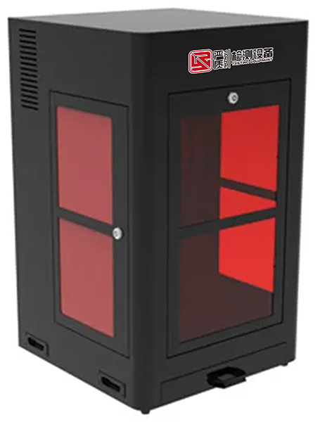
Optical aging stability test box Model: CHT-1800
Steady-state simulation test box Model: CHT-WTBBA
UV accelerated aging test box Model: CHT-UVDC28
Current Continuity Test System Model: CHT-11D
Diode Thermal Performance Test System Model: CHT-12D
Pulse voltage test system Model: CHT-14D
PV Module Salt Spray Corrosion Test Chamber:CHT-16D
Optical senescence test box / photovoltaic module test LID: CHT-18D
Insulation withstand voltage tester Model: CHT-2813W
Wet leakage test system Model: CHT-3621W
Outdoor sun exposure test system model: CHT-H206
Dynamic Load Test Machine Model: CHT-20D
Static load test machine model: CHT-26D
PID Test System Model: CHT-PID
Component crushing tester Model: CHT-30D
Grounding continuity Tester Model: CHT-2813W
Lead end strength test machine Model: CHT-31
Appearance table Model: CHT-W26
Drop ball impact test machine Model: CHT-10
Photovoltaic welding strip stripping force testing machine
photovoltaic welding strip stripping force integrated machine
Universal material testing machine
Photovoltaic glass four-point bending test machine model: CHT-4 WQJN
Crosslinking degree test System Model: EVA-CC
2nd element image instrument model: CHT-3020
Two-dimensional image instrument
Acetic acid test box Model: CHT-YW 400
High pressure Accelerated aging test box Model: CHT-HAST-800
Differential Scanning Calorimeter (DSC) Model: CHT-CS300
Spectrophotometer Model: CHT-3400
Fourier transform infrared spectrometer model: CHT-H8030
Photovoltaic welding strip stripping force testing machine
Photovoltaic welding strip stripping force integrated machine
Universal material testing machine
Full-spectrum Ellipsometer Model: CHT-TP 01
Water vapor transmission and filtration rate Model: CHT-40B
No-rotor vulcanizer model: CHT-LH 06
Atomic force microscope Model: CHT-AFM
Solar cell TLM grid line contact resistance analyzer model: CHT-6070 TLM
Battery cell light aging box Model: CHT-DCPBBA
Photovoltaic cell PL detector model: CHT-80D
Scan four-probe square resistance meter Model: CHT-4500 RH
- About Us
- Contact Us
- CN


 400-9662-958


 Location: